What power electronics does
Dr. Xu's one-line description is "a course on solid-state converters and digital control" (intro slide 2). Mohan says the same thing longer: power electronics processes and controls the flow of electric energy, handing the load the voltage and current in the form it needs (Mohan 1-1).
Mohan Fig. 1-1. The controller compares the output with a reference and adjusts the switches. Dr. Xu draws the same idea on Ch. 1 slides 9 to 12.
From milliwatts to megawatts (intro slides 11 to 23)
- Motor speed control (class note: VFD, variable-frequency drive): robots to pumps.
- Switch-mode power supplies: computers, telecom, instruments. Small size, high efficiency, high power density.
- Electronic ballasts, wind (class note: also solar and other renewable energy) and fuel cells.
- UPS: hospitals, satellite control. Topology: converter + batteries + inverter (intro slide 19).
- EV and PHEV, and aerospace (intro slide 20: 787 at 1 MW of electric power, all-electric aircraft at 2 MW).
- Utilities: HVDC links two grids, 1000 MW and up, over 1000 km (intro slide 22); static var compensators adjust reactive power with no rotating parts (intro slide 23).
Intro slides 1 to 10 (outline, textbook, labs, marking) are course admin and aren't covered here.
Operated like a switch
Ch. 1 slide 2 opens with one line: "The devices are operated like a switch." The hero demo shows why. Put a transistor in series with a load and let it sit part-way on, like the pass transistor in a linear supply (Mohan 1-2). Step through the numbers.
- The transistor and the load share the source: $$v_T = V_d - i_TR$$ This is the load line. "How far on" just slides the operating point along it.
- Power in the transistor: $$p_T = v_T\,i_T = (V_d - i_TR)\,i_T$$
- It's zero at both ends: off ($i_T = 0$) and fully on ($v_T = 0$). Set $\frac{dp_T}{di_T} = V_d - 2i_TR = 0$: the worst point is halfway, $i_T = \frac{V_d}{2R}$, where $$p_{T,\max} = \frac{V_d^2}{4R} = \frac{48^2}{4\times2.4} = 240\ \text{W}$$ The load gets 240 W too, so the efficiency is 50%.
- So a converter never parks a device in between. Ch. 1 slide 8: "these devices will be either turned on (shorted) or turned off (open circuit). They NEVER operate in active mode."
The ideal switch
Slide 8 then idealizes every device: when on, the saturation voltage is zero; when off, the leakage current is zero. Mohan 2-4 adds two more ideal properties: it switches instantly, and it needs no power from the gate driver. Real devices break each one a little, and those small breaks are the losses on the bench in section 06.
Three kinds of switch (Mohan 2-1)
Mohan sorts every power device by how much the gate controls. Dr. Xu's slides cover the last two groups. Bold lines are the idealized characteristics: on is the vertical axis (current, no voltage), off is the horizontal axis (voltage, no current).
Diode
No control. The circuit turns it on and off: it conducts when forward biased (about 1 V drop), blocks reverse voltage. Every converter's freewheeling diode. Not on Dr. Xu's slides (Mohan 2-2).
Thyristor
Half control. The gate latches it on; only the circuit turns it off. SCR, and the GTO/GCT that adds gate turn-off. Ch. 1 slides 3 to 4.
Controllable switch
Full control. The gate turns it on and off. IGBT, MOSFET (slides 5 to 6), and the older BJT, which needs a steady base current $I_B > I_C/h_{FE}$ with $h_{FE}$ only 5 to 10 (Mohan 2-5). The IGBT replaced it.
A 48 V source feeds a 2.4 Ω load through a transistor. Where along its range does the transistor get hottest?
$p_T = v_Ti_T$ needs both at once. Fully on, $v_T \approx 0$; fully off, $i_T \approx 0$; either way $p_T \approx 0$. Halfway you get $24\times10 = 240$ W, the peak $\frac{V_d^2}{4R}$. That's why converters only ever use the two ends.
Thyristors: SCR and GTO/GCT
SCR, the silicon-controlled rectifier, is the thyristor. Current flows from anode to cathode ($i_a$, with $V_T$ across it). To turn it on, $i_g > 0$: a short pulse is enough, because once it conducts it latches and the gate can be removed (Mohan 2-3). To turn it off, make $V_T < 0$: a reverse voltage drives $i_a$ to zero, and only then is the SCR off. Slide 3's warning: a negative $i_g$ will not turn it off.
Ratings (slide 3): $i_a$ from 10 A to 6000 A, $V_T$ from 50 V to 6500 V, up to 500 Hz. Main use: ac-dc converters (rectifiers). That isn't a coincidence. An ac line reverses $V_T$ every half cycle, so it turns the SCR off for free. In class, Dr. Xu circled the 6500 V and wrote LTT for higher voltage (light-triggered thyristor), about 10 kV: fired by light through an optical fibre, which is how HVDC valves with many thyristors in series are triggered (Mohan 2-3).
GTO and GCT: a thyristor you can turn off
Same symbol plus a gate turn-off mark. On with $i_g > 0$, off with $i_g < 0$. Both directions are gate current, so it's a current-controlled device. Mohan 2-7: the negative gate current has to be large, typically as much as a third of the anode current, for a few microseconds, and a snubber across the device limits $dv/dt$ at turn-off. Ratings (slide 4): 10 A to 6000 A, 50 V to 6000 V, up to 1 kHz. Main use: high-power dc-ac converters (inverters). In class: the GTO is out of industry, and the GCT (gate-commutated thyristor) is active in MV converters.
Slides 3 and 4 give the range $i_a$ = 10 A to 6000 A for both the SCR and the GTO/GCT. The slide 7 table gives the single-device commercial rating as 4500 A for both. If an exam asks for the rating, quote the table (SCR 4500 A/6500 V, GTO/GCT 4500 A/6000 V) and say it's the table's number; if it asks for the range, quote 10 A to 6000 A.
An SCR on a dc supply is conducting 100 A. You remove its gate current. What happens?
Once an SCR conducts it's latched, and the gate has no more say. Removing $i_g$, or even making it negative, changes nothing. It turns off only when the circuit drives $i_a$ to zero with $V_T < 0$. On a dc supply that never happens by itself, so this SCR stays on.
Why can't a plain SCR be the switch in a buck converter fed from a battery?
A buck has to turn its switch off every period. An SCR only turns off when $V_T < 0$ drives $i_a$ to zero, and a battery never reverses. A negative gate current won't help either. So dc-dc and dc-ac jobs need a device with gate turn-off: GTO/GCT, IGBT or MOSFET.
IGBT and MOSFET: voltage control
IGBT, insulated gate bipolar transistor: collector C, emitter E, gate G. On with $V_{GE} > 0$, off with $V_{GE} < 0$. It's voltage-controlled: the gate is insulated, so $i_G = 0$ at steady state. Current only flows briefly to charge or discharge the gate capacitance at each switching edge. Ratings (slide 5): up to 1200 A/4500 V, up to 20 kHz. Main use: dc-ac converters (inverters).
Dr. Xu's class notes on slide 5 update those numbers: he crossed out 4500 V and wrote $V_{CE,BR}$ about 6 kV, $I_{C,DC}$ about 800 A per die, circled 20 kHz and wrote 50 kHz, and several kW to MW for the power range. IGBTs now come in silicon and SiC. He also drew the gate driver as a pulse source wired from gate to emitter: $V_{GE}$ is measured from the gate to the emitter, not to ground.
Power MOSFET, drain D, source S, gate G. N-channel: on with $V_{GS} > 0$, off with $V_{GS} < 0$. P-channel: the reverse, on with $V_{GS} < 0$, off with $V_{GS} > 0$. Class notes: N-channel for higher power, P-channel for lower-power, small applications. Ratings (slide 6): up to 150 A/1000 V (circled in class: that's the silicon MOSFET), up to 200 kHz. Main use: dc-dc converters (switch-mode supplies). In class he added SiC and GaN MOSFETs beside it.
Why the MOSFET is the fast, low-voltage one (Mohan 2-6): it switches in tens to hundreds of nanoseconds, but its on-state resistance climbs steeply with its voltage rating, $r_{DS(on)} = k\,BV_{DSS}^{2.5\text{ to }2.7}$ (Mohan eq. 2-9), so a high-voltage MOSFET has high conduction loss. The IGBT keeps a low on-state voltage (2 to 3 V in a 1000 V device, Mohan 2-8) even at high voltage ratings, which is why it takes over where the slide 7 MOSFET row stops. Mohan's Table 2-1 sums it up: MOSFET low power, fast; IGBT medium power, medium speed; GTO high power, slow.
Slides 5 and 6 say "to turn it off, $V_{GE} < 0$" (and $V_{GS} < 0$). Physically, any gate voltage below the threshold (a few volts) turns an IGBT or N-channel MOSFET off, so 0 V works. Drivers often use a negative voltage anyway (for example −5 V to −15 V, common with IGBTs and SiC MOSFETs) for noise margin and faster turn-off. On the exam, write the slide's rule: on with $V_{GE} > 0$, off with $V_{GE} < 0$.
How do you turn on a P-channel power MOSFET?
P-channel is the mirror image of N-channel: on with $V_{GS} < 0$, off with $V_{GS} > 0$ (slide 6). Both are voltage-controlled, so a gate current pulse is the thyristor's language, not the MOSFET's.
The ratings table and the rules
Slide 7 puts the four devices side by side. Read down the table: the frequency goes up and the ratings come down. Memorize it; it isn't on the formula sheet.
| Switching device | Single-device rating (commercial) | Operating frequency (commercial) | Gate control | Main use |
|---|---|---|---|---|
| SCRClass: LTT to about 10 kV | 4500 A / 6500 V | 500 Hz | Current | ac-dc (rectifiers) |
| GTO/GCTClass: GTO out of industry, GCT in MV converters | 4500 A / 6000 V | 1 kHz | Current | high-power dc-ac (inverters) |
| IGBTClass: about 6 kV, 800 A per die, 50 kHz; Si and SiC | 1200 A / 4500 V | 20 kHz | Voltage | dc-ac (inverters) |
| Power MOSFETClass: SiC MOSFET to about 500 kHz, GaN MOSFET to about 5 MHz | 150 A / 1000 V | 200 kHz | Voltage | dc-dc (switch-mode supplies) |
In class Dr. Xu bracketed all four rows "Si": the table is for silicon devices. The SiC and GaN frequencies are his red notes at the top of slide 7. Mohan (2002) quotes older numbers (IGBT modules to 1700 V/1200 A, GTOs to 4.5 kV at a few hundred Hz to 10 kHz); on the exam, use Dr. Xu's table.
The summary slide (slide 8), five rules
- SCR and GTO/GCT are current-controlled: the gate current turns them on. An SCR can NOT be turned off with a negative gate current.
- IGBT and power MOSFET are voltage-controlled: the gate voltage turns them on and off.
- They never operate in active mode: fully on (shorted) or fully off (open).
- All of them are unidirectional, and all are modelled as ideal switches: zero saturation voltage on, zero leakage current off.
- Increase the switching frequency, decrease the device rating. Section 06 shows why.
The controlled current flows one way only (anode to cathode, collector to emitter, drain to source in an N-channel). That's why converters add a diode in antiparallel wherever reverse current must flow. Real power MOSFETs also have an internal body diode that conducts in reverse, and the ideal model ignores it. On the exam, treat all four as unidirectional, as the slide does.
- Name the converter. A dc source never reverses $V_T$, so dc-dc and dc-ac need gate turn-off. On an ac line an SCR turns off by itself.
- Voltage the switch blocks: $V_d$ in a chopper or an inverter leg; the peak line voltage $\sqrt{2}\,V_{LL}$ in a three-phase bridge.
- Peak current it carries: $I_{\max}$ in a chopper; $\sqrt{2}$ times the rms line current $\frac{S}{\sqrt{3}V_{LL}}$ in a three-phase inverter.
- Switching frequency: $f_s$, or the line frequency for a rectifier.
- Pick the row of the slide 7 table that covers all four, with the device's main use as the tie-break. If only the current is too high, put devices in parallel. Give a one-line reason for each number.
Each box reaches from zero up to a device's rating and across to its frequency limit. The dot is the job. Dashed boxes: SiC and GaN, whose frequencies are from class but whose ratings weren't given, so the silicon MOSFET's 150 A/1000 V stands in.
A dc-dc converter needs a switch that blocks 400 V and carries 30 A at 100 kHz. From the slide 7 table?
Only the MOSFET reaches 100 kHz (200 kHz in the table); 400 V and 30 A are inside its 1000 V and 150 A. The IGBT tops out at 20 kHz, the GTO/GCT at 1 kHz, and the SCR can't turn off on dc at all. Load "400 V, 30 A, 100 kHz dc-dc" into the selector to see every row.
Why faster means smaller: switching loss
Slide 8's last rule, "increase switching frequency, decrease device rating", comes from what happens during the edges. Mohan 2-4 uses the circuit that sits inside every converter: the switch carries an inductor's current, which is held at $I_o$, and a diode takes that current whenever the switch is off. When the switch is off it blocks $V_d$.
Mohan Fig. 2-6a, the clamped-inductive switching circuit. The current source stands in for the inductor current. The diode is ideal.
Real edges take time. Turning on, the current has to rise all the way to $I_o$ before the diode can let go, so the switch voltage stays at $V_d$ the whole time. Only then does the voltage fall. Turning off is the mirror image. Step through it.
- Turn-on: current rise $t_{ri}$ at $v_T = V_d$, then voltage fall $t_{fv}$ at $i_T = I_o$: $$t_{c(on)} = t_{ri} + t_{fv} \quad (2\text{-}1)$$
- The power $p_T = v_Ti_T$ is a triangle that peaks at $V_dI_o$. During $t_{ri}$ the area is $\frac{1}{2}V_dI_ot_{ri}$; during $t_{fv}$ it's $\frac{1}{2}V_dI_ot_{fv}$ (taking $V_{on} \approx 0$). Add them: $$W_{c(on)} = \tfrac{1}{2}V_dI_ot_{c(on)} \quad (2\text{-}2)$$
- Turn-off: the voltage rises first ($t_{rv}$), because the diode can't take the current until $v_T$ reaches $V_d$. Then the current falls ($t_{fi}$): $$t_{c(off)} = t_{rv} + t_{fi}, \qquad W_{c(off)} = \tfrac{1}{2}V_dI_ot_{c(off)} \quad (2\text{-}4,\ 2\text{-}5)$$
- There are $f_s$ turn-ons and $f_s$ turn-offs every second: $$P_s = \tfrac{1}{2}V_dI_of_s\left(t_{c(on)} + t_{c(off)}\right) \quad (2\text{-}6)$$ Linear in $f_s$ and linear in the switching times.
- While it's on, the switch drops $V_{on}$ (about a volt): $$P_{on} = V_{on}I_o\frac{t_{on}}{T_s} \quad (2\text{-}7)$$ Off-state leakage is negligible, so the total is $P_T = P_s + P_{on}$.
- Now slide 8's rule. A device can only shed so much heat, $P$. Ignoring conduction, $$V_dI_o \le \frac{2P}{f_s\left(t_{c(on)} + t_{c(off)}\right)}$$ Double $f_s$ and you halve the $V_dI_o$ the device can switch. And big, high-voltage, high-current devices switch slowly (bigger $t_c$), which pushes them down to low frequencies. Both effects point the same way: higher frequency, lower rating.
Neither $P_s$ nor $P_{on}$ is on the F2026 sheet, and neither appears on Dr. Xu's Sept 8 slides; they're Mohan's, and they explain his slide 8 rule. The Sept 15 lecture (slide 25) uses the same idea: raising $f_s$ cuts the output ripple but raises the switching loss and lowers the efficiency. If you can draw the triangle, you can rebuild $P_s$ in two lines.
The time axis is broken like Mohan's Fig. 2-6b: both edges are zoomed in to the same scale, and the long on and off stretches are squeezed.
Same switch, same $V_d$, $I_o$ and duty cycle. You double $f_s$. What happens to the losses?
The energy per edge doesn't change, but there are twice as many edges per second, so $P_s \propto f_s$ doubles. $P_{on} = V_{on}I_o\frac{t_{on}}{T_s} = V_{on}I_oD$ depends on D, not $f_s$. Try it: load "Mohan P2-1 · 25 kHz", then "100 kHz": 6.75 W becomes 27 W.
Four converter families
A converter is named by what goes in and what comes out. In every one, the input is usually fixed and the output is adjustable and regulated by a controller (slide 13).
dc-dc converter (slide 9)
- Buck, boost, Cuk, flyback, forward, push-pull.
- Main functions: adjustable dc output, good regulation.
- Usual switch: MOSFET.
ac-dc converter, rectifier (slide 10)
- Main functions: ac to dc, adjustable dc output.
- Usual switch: SCR (diodes if the output needn't be adjustable).
dc-ac converter, inverter (slide 11)
- Main functions: dc to ac, adjustable magnitude and frequency.
- Usual switch: IGBT (GCT at the highest power).
ac-ac converter (slide 12)
- Direct ac to ac, no dc stage. Class note: cycloconverter and matrix converter.
- Not studied in ELE754.
- $V_o \le V_i$ always: buck.
- $V_o \ge V_i$ always: boost.
- $V_o$ has to go both below and above $V_i$: buck-boost or Cuk.
Slide 13's conclusions: the input voltage and frequency are usually fixed, the output is usually adjustable and regulated, and ELE754 studies the three families industry uses most: dc-dc, ac-dc and dc-ac. That is also the order of the course (intro slides 5 to 6): dc-dc converters first, starting with buck and boost next lecture, then diode and thyristor rectifiers, then inverters.
In:
Out:
During an outage, a hospital UPS runs its 120 V, 60 Hz loads from a battery bank. Which family does that last stage belong to?
Battery (dc, fixed) in, 60 Hz ac out: an inverter. Intro slide 19 gives the full UPS topology as converter + batteries + inverter: a rectifier charges the battery from the grid, and the inverter feeds the load.
Practice in Dr. Xu's style
There's no past exam question on this lecture, so these are practice questions written in the style of his exams (scenario, numbered parts, marks, units). They are not real exam questions. P1 reuses the real circuits and numbers from last year's midterm and final; P2 is Mohan's Problem 2-1 with a conduction loss added. Do P1 (about 12 min) and P2 (about 12 min) on the practice pages of your notes, trying each part before you reveal it. P3 is extra if you have time.
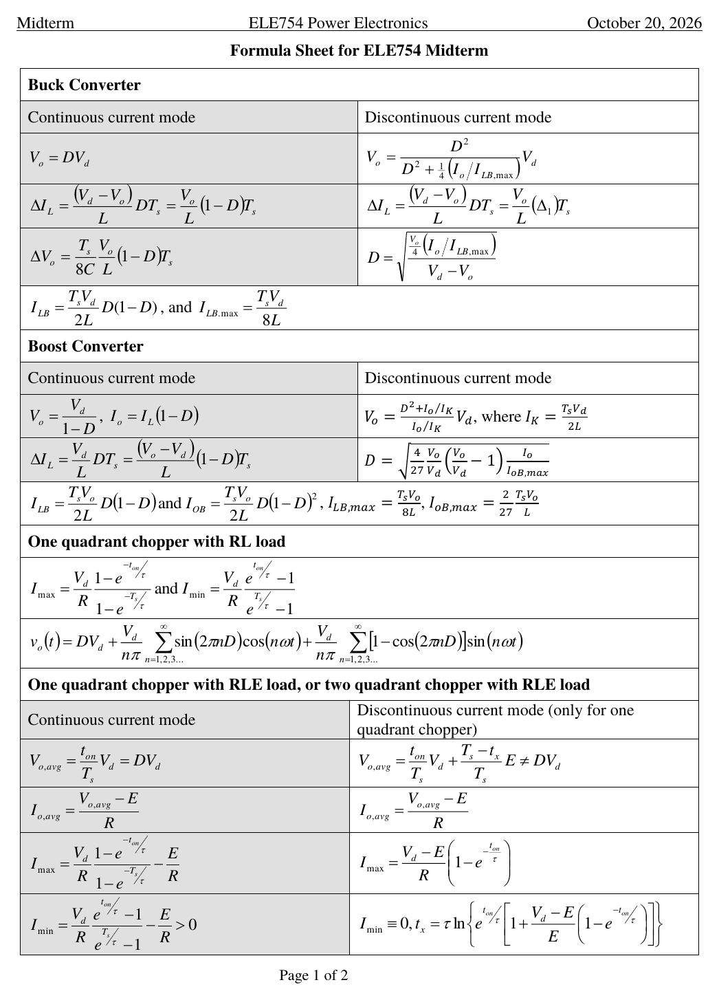
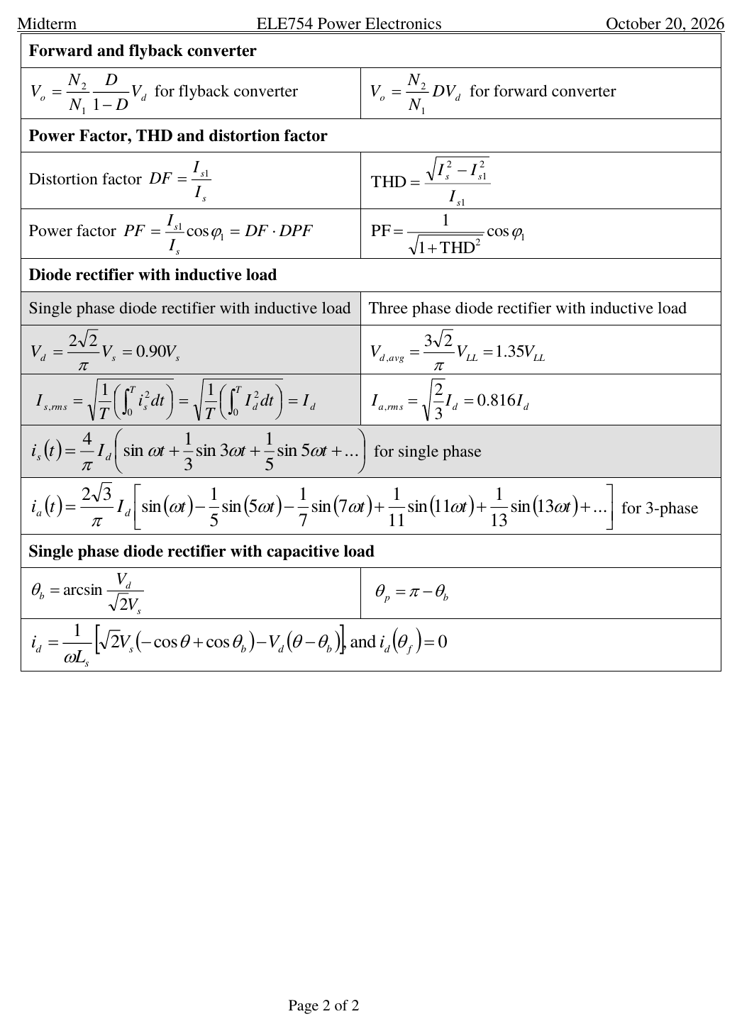
It's the F2026 midterm sheet, organized by converter family, the same families as section 07.
- Page 1, dc-dc: buck and boost (CCM and DCM), the one-quadrant chopper with an RL load, and the chopper with an RLE load.
- Page 2, dc-dc then ac-dc: forward and flyback, then power factor, THD and distortion factor, then diode rectifiers with inductive and capacitive loads.
- No dc-ac rows (inverters aren't on the midterm), and nothing from this lesson: the ratings table, the gate rules, the selection procedure and $P_s$, $P_{on}$ are all memory work.
Question P1 (practice, 15%) Switching devices · about 12 min
Three converters from last year's exams:
- (a) F2025 midterm Q2: a one-quadrant chopper feeds a dc motor from $V_d = 200$ V at $f_s = 1$ kHz. Its armature current peaks at $I_{\max} = 49.0$ A (from that question's DCM solution).
- (b) F2025 final Q3: a three-phase full-bridge thyristor rectifier drives a 100 kW dc motor (back emf $E_o = 750$ V) from a 600 V, 60 Hz line.
- (c) F2025 final Q4: a 1.5 MVA grid-side inverter for a wind turbine, $V_d = 1250$ V dc link, 690 V ac side, switching at 1080 Hz.
- (a) dc to dc: a dc-dc converter (a step-down chopper). (b) 60 Hz ac to adjustable dc: an ac-dc converter, rectifier. (c) dc link to 60 Hz grid ac: a dc-ac converter, inverter.
Hint: work out the voltage each switch blocks and the peak current it carries first.
- (a) Blocks 200 V, carries 49.0 A, at 1 kHz, and needs gate turn-off (dc input). Power MOSFET (150 A/1000 V, 200 kHz) or IGBT (1200 A/4500 V, 20 kHz) both fit. The F2025 midterm used an IGBT. The SCR is out: no gate turn-off.
- (b) Each thyristor in a three-phase bridge blocks up to the peak line voltage, $\sqrt{2}\times600 = 848.5$ V. The motor current is $I_a = \frac{P_{out}}{E_o} = \frac{100\text{ kW}}{750\text{ V}} = 133.3$ A, at 60 Hz. SCR: 4500 A/6500 V, 500 Hz, and its main use is exactly this. The ac line reverses $V_T$ every cycle, so it turns off by itself.
- (c) Rated current $I = \frac{S}{\sqrt{3}V_{LL}} = \frac{1.5\text{ MVA}}{\sqrt{3}\times690} = 1255$ A rms, so the peak is $\sqrt{2}\times1255 = 1775$ A. Each switch blocks $V_d = 1250$ V at 1080 Hz with gate turn-off.
- (c) continued. The IGBT is right on voltage (4500 V) and frequency (20 kHz) but one device is only 1200 A, so use two in parallel (or a module built from paralleled dies; class: about 800 A per die). The GTO/GCT has the current but 1080 Hz is past its 1 kHz table limit. (a) MOSFET or IGBT, (b) SCR, (c) IGBTs in parallel.
- The chopper's source is dc, so nothing ever makes $V_T < 0$ to bring $i_a$ to zero, and a negative $i_g$ won't turn an SCR off. Once fired, it would stay on.
- IGBT: the gate driver connects between gate and emitter (Dr. Xu's class drawing). On: $V_{GE} > 0$. Off: $V_{GE} < 0$. $i_G = 0$ at steady state.
Question P2 (practice, 15%) Switching and conduction loss · about 12 min
A switch in the clamped-inductive circuit of Mohan Fig. 2-6a switches $V_d = 300$ V and $I_o = 4$ A. Its datasheet gives $t_{ri} = 100$ ns, $t_{fv} = 50$ ns, $t_{rv} = 100$ ns, $t_{fi} = 200$ ns, and $V_{on} = 2$ V. It runs at $D = 0.5$. (Mohan Problem 2-1, with an on-state voltage added.)
- $t_{c(on)} = t_{ri} + t_{fv} = 150$ ns and $t_{c(off)} = t_{rv} + t_{fi} = 300$ ns.
- $W_{c(on)} = \frac{1}{2}V_dI_ot_{c(on)} = \frac{1}{2}\times300\times4\times150\text{ ns} = $ 90 µJ; $W_{c(off)} = $ 180 µJ.
- $P_s = f_s\left(W_{c(on)} + W_{c(off)}\right) = f_s\times270\ \mu$J.
- 25 kHz: 6.75 W. 100 kHz: 27 W. Four times the frequency, four times the loss.
- $P_{on} = V_{on}I_o\frac{t_{on}}{T_s} = 2\times4\times0.5 = $ 4 W, the same at any $f_s$.
- $P_T = P_s + P_{on} = 27 + 4 = $ 31 W. At 100 kHz the edges cost almost seven times the conduction.
- Conduction takes 4 W whatever the frequency, leaving 11 W for switching.
- $f_{s,\max} = \frac{11\text{ W}}{270\ \mu\text{J}} = $ 40.7 kHz
- With 11 W for switching, $V_dI_o \le \frac{2P}{f_s(t_{c(on)} + t_{c(off)})}$: 1956 V·A at 25 kHz but only 489 V·A at 100 kHz. Four times the frequency, a quarter of the voltage times current the same device can switch.
- And devices built for more voltage and current switch more slowly (bigger $t_c$), so they're stuck at low $f_s$: SCR 500 Hz, MOSFET 200 kHz.
Question P3 (practice, 10%) Short answers · Extra if you have time
- Nothing: a negative $i_g$ will not turn an SCR off (slide 3). Apply a reverse voltage, $V_T < 0$, so $i_a$ falls to zero; then it's off. Turning off with $i_g < 0$ is what the GTO/GCT adds.
- In the active region the device has voltage across it and current through it at the same time. Halfway: $v_T = 24$ V, $i_T = 10$ A, so $p_T = 240$ W while the load gets 240 W: 50% efficiency.
- Fully on ($v_T \approx 0$) or fully off ($i_T \approx 0$) gives $p_T \approx 0$. Slide 8: "They NEVER operate in active mode." Ideal switch: zero voltage on, zero leakage off.
- N-channel: on $V_{GS} > 0$, off $V_{GS} < 0$. P-channel: on $V_{GS} < 0$, off $V_{GS} > 0$. Both voltage-controlled. N-channel for higher power, P-channel for lower-power small applications (class note).
Traps that cost marks
- "A negative gate current turns an SCR off." It doesn't. Only $V_T < 0$, driving $i_a$ to zero. Gate turn-off with $i_g < 0$ is the GTO/GCT.
- Mixing the control types. SCR and GTO/GCT: gate current. IGBT and MOSFET: gate voltage ($V_{GE}$, $V_{GS}$), with $i_G = 0$ at steady state.
- P-channel MOSFET backwards: it turns on with $V_{GS} < 0$.
- An SCR for a dc-dc or dc-ac job. On a dc source it can never turn off.
- Quoting 6000 A as the SCR's single-device rating. The slide 7 table says 4500 A/6500 V; 10 A to 6000 A is the range on slide 3. Say which one you mean.
- Hz and kHz in the table: SCR 500 Hz, GTO/GCT 1 kHz, IGBT 20 kHz, MOSFET 200 kHz.
- "Switching loss doesn't depend on frequency." $P_s = \frac{1}{2}V_dI_of_s(t_{c(on)} + t_{c(off)})$ is linear in $f_s$; $P_{on}$ isn't.
- Calling it a buck when the output has to go above and below the input. That's a buck-boost (or Cuk).
- Nothing from this lesson is on the formula sheet: the table, the gate rules and $P_s$ are memory work. And units: the cover page says marks are lost without them.
Drill it in chat
Go back to the chat and say "quiz me on switching devices". You get one question at a time, and I'll fix exactly where your reasoning breaks.
Then the grill
grill.pierrek.ca · ELE754 sections "L1: Switching devices & converter types" (9 questions) and "Formula sheet (F2026): find it, use it, know what's missing" (10).